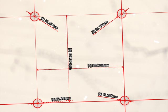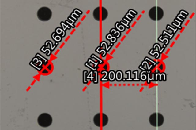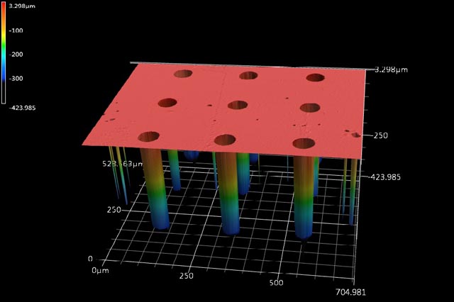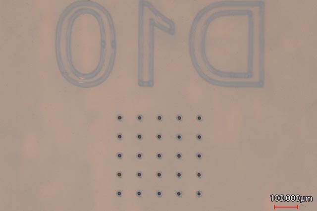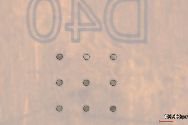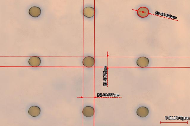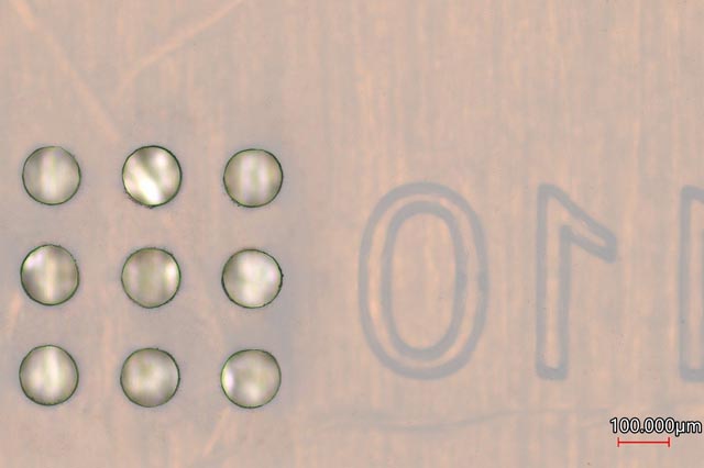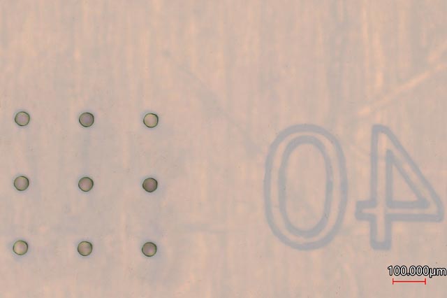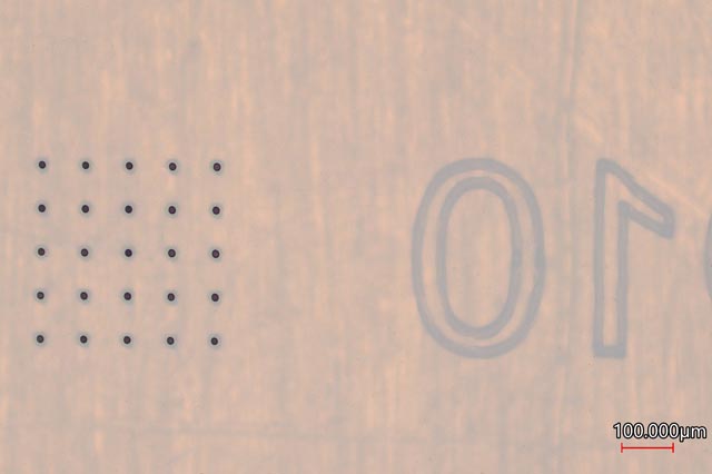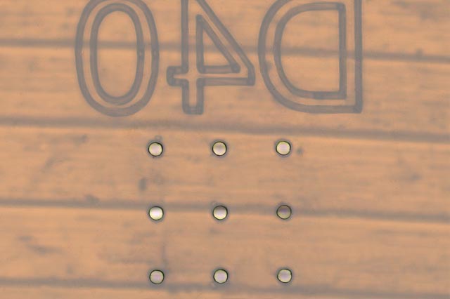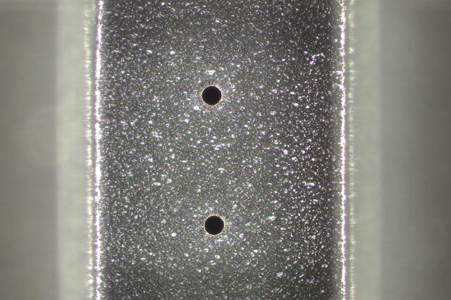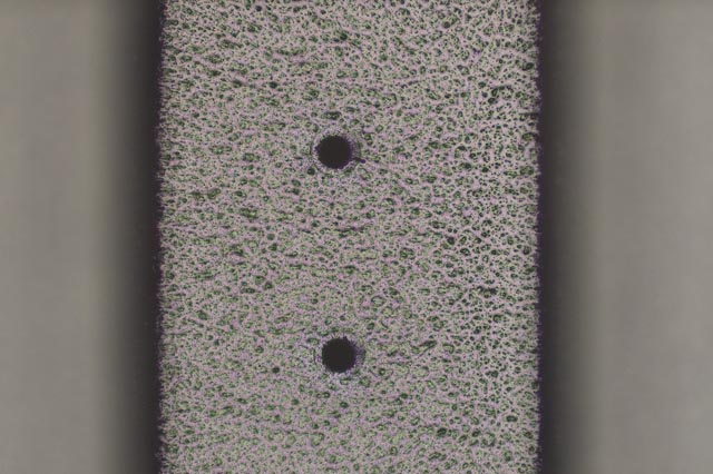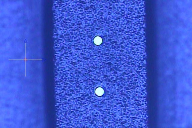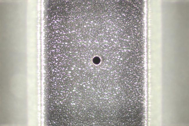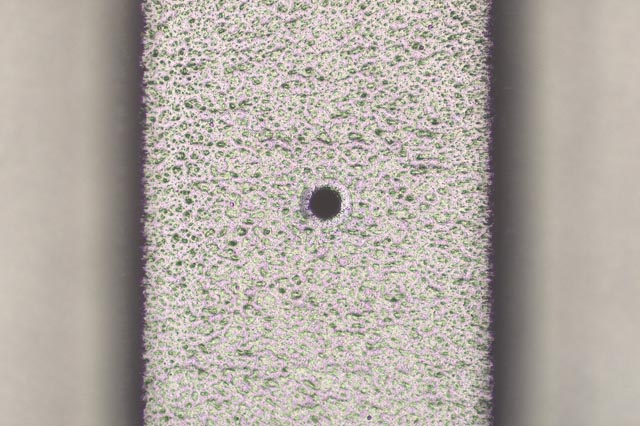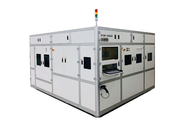
Product | Drilling Machine
Model: Laser Drilling Equipment/SCM-A322
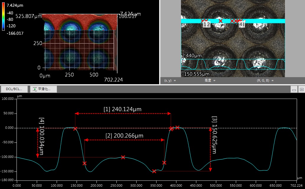
● The difference in diameter between the upper and lower openings can be controlled to <30 μm.
● The workable compound thickness can reach 1,000μm.
● Operation accuracy <±10 μm, Cpk >1.67.